The communication range, sensitivity, and interference immunity of wireless RF devices depend primarily on the antenna PCB layout design. Most RF performance issues stem from non-standard antenna layout, clearance, grounding, and impedance design. This article provides a simplified overview of general RF antenna design guidelines, routing and grounding techniques, as well asCeramic Surface-Mount Antennas, FPC Flexible Antennas, LDS Laser Direct Structuring AntennasDedicated layout solutions for three common types of antennas, compatible with mainstream RF scenarios such as 2.4 GHz, 5 GHz, Bluetooth, Wi-Fi, and Sub-G, designed to meet the needs of rapid engineering design and help avoid pitfalls during mass production.
I. Three Core General Guidelines for Antenna Layout
The following rules apply to all on-board RF antennas—including those on ceramic, FPC, and LDS boards—and form the basis for ensuring antenna performance.
1.1 3D Full-Dimensional Clearance Guidelines (Core Red Line)
All types of metal interference are strictly prohibited within the antenna radiation zone; a three-dimensional clear zone spanning the entire PCB must be established, with absolutely no room for design compromises:
- Clearance from the Surface: No metal structures—including components, copper traces, shielding covers, screws, etc.—may be placed within the antenna radiation pattern;
- Interlayer Clearance: The inner layer and bottom layer corresponding to the antenna projection must be completely hollowed out; no plating, routing, or fixed vias are permitted in these areas;
- Clearance: The distance between the antenna and the metal structure of the entire unit must be ≥λ/10; the minimum clearance distance for the 2.4 GHz band must be ≥12.5 mm to prevent radiation distortion and standing wave ratio (SWR) degradation.
Only the antenna feed point and the matching circuit area may be laid out normally; the rest of the radiation area must be kept strictly clear.
1.2 Continuity Criteria for 50 Ω Impedance
RF feedlines and matching networks must maintain a standard characteristic impedance of 50 Ω throughout their entire length, and the trace width and dielectric thickness must be uniform and consistent. Sudden changes in width, 90° right-angle bends, branching traces, and frequent layer changes are prohibited to prevent issues such as signal reflection, reduced radiation efficiency, and excessive VSWR caused by impedance discontinuities.
1.3 Guidelines for the Isolation of Digital and Analog Zones
Strictly separate the RF antenna area, RF circuit area, digital circuit area, and power supply area, ensuring that these areas do not overlap. Digital clock and power switch noise are the primary sources of RF interference; isolating these areas can effectively reduce the antenna’s background noise and prevent device lag, packet loss, and reduced communication range.
II. Guidelines for Overall PCB Zone Layout
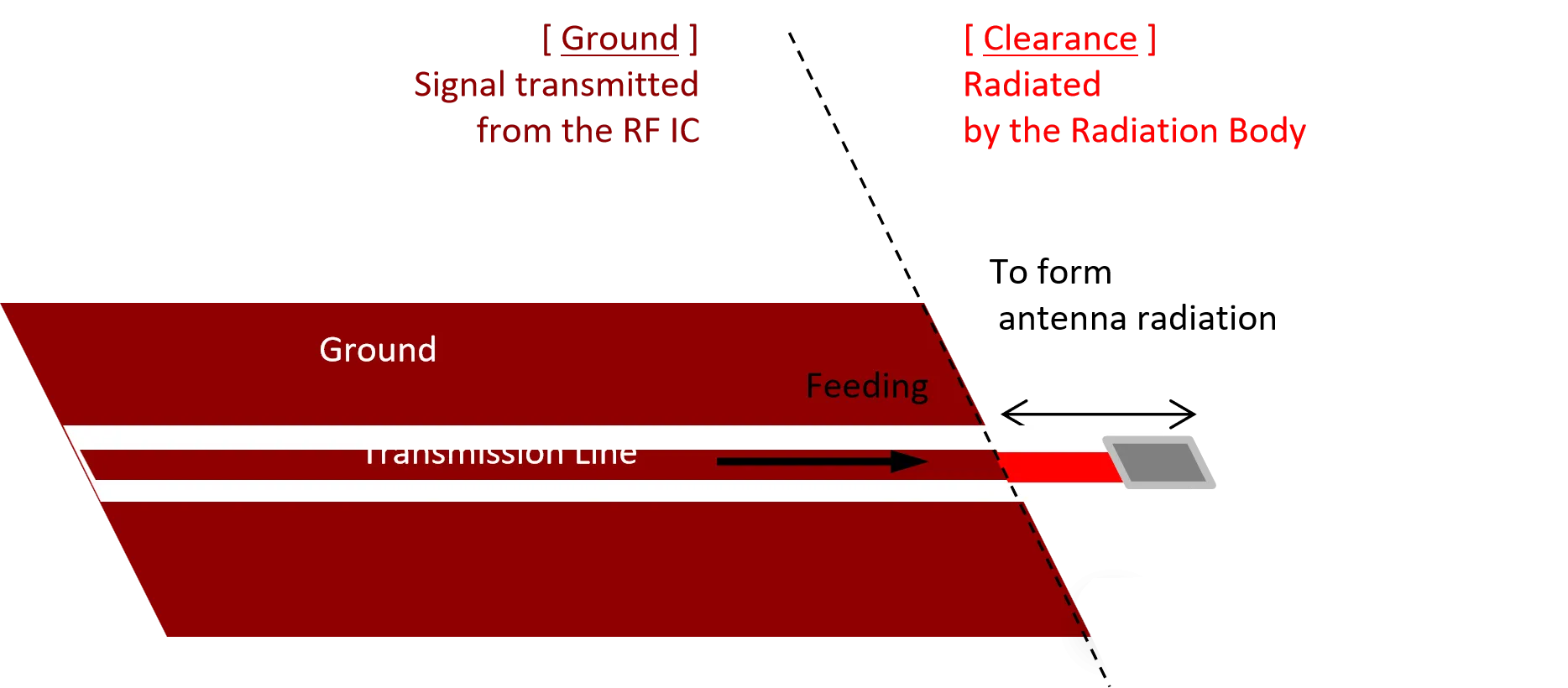
Generally followAntennas on the edge, RF components grouped together, digital electronics kept at a distance, and power supplies isolatedThe principles of minimalist layout.
2.1 Antenna Site Selection
All three types of antennas should preferably be placed along the edges of the PCB or in open corners of the finished unit to minimize obstruction and absorption by the PCB substrate and copper foil. They must not be placed in the center of the PCB, as the dense concentration of traces and components in that area will severely attenuate the RF signal.
2.2 Logic of Feature Layout
Arrange components uniformly in a unidirectional layout following the sequence: “Antenna Radiation Area → Matching Network Area → RF Chip Area → Digital/Power Area.” Place the matching circuit immediately adjacent to the antenna feed point to shorten RF trace lengths and reduce losses; concentrate the digital and power circuits on the opposite side of the PCB to achieve electromagnetic shielding through a solid layer.
III. Minimal Design Guidelines for Feeder and Matching Networks
3.1 50Ω Feeder Cabling Requirements
- Shortest Direct Connection: Short, straight wiring with no redundant loops, reducing transmission loss and parasitic parameters;
- Avoid right-angle bends: Use rounded bends or 45° beveled bends, and eliminate 90° right-angle bends;
- No branching traces: A single main trace throughout, with no redundant branches or test pads;
- Prioritize routing on the same layer: Avoid changing layers whenever possible; when a layer change is necessary, ensure precise impedance matching for the vias.
3.2 Matching Network Design
The native impedance of all three types of antennas is not the standard 50 Ω; therefore, a π-type three-element matching network (two capacitors and one inductor) must be included to provide impedance tuning and harmonic suppression.
The matching circuit is laid out close to the feed point, with routing kept to a minimum, and high-frequency RF-specific components are used; no clearance is required in this area, allowing for normal ground plane placement, which improves circuit stability.
IV. Grounding and Strata: Core Processes
4.1 Layered Formation Design
The ground plane for RF must be fully copper-plated with no cutouts or gaps to provide a stable reference ground for RF traces; stacking digital or power traces on top of it is prohibited.
Strictly separate the areas: The soil layer directly beneath the antenna’s radiation zone is completely removed, while the soil layer beneath the RF circuitry and matching network remains intact, thereby achieving “radiation without soil, circuitry with stable grounding.”
4.2 Key Points of Grounding Procedures
- Densification of via placement: Densely place ground vias for RF ground and matching circuit ground with a spacing of ≤3 mm to reduce ground impedance;
- Layer Stitching: Stitching vias are arranged at the edges of the RF region to connect through all layers, thereby suppressing edge radiation interference;
- Single-point grounding: The RF ground is connected to the digital ground and the power ground at a single point, eliminating ground loops and preventing noise from entering the RF link.
V. Streamlined Layout Solutions for Three Types of Antennas
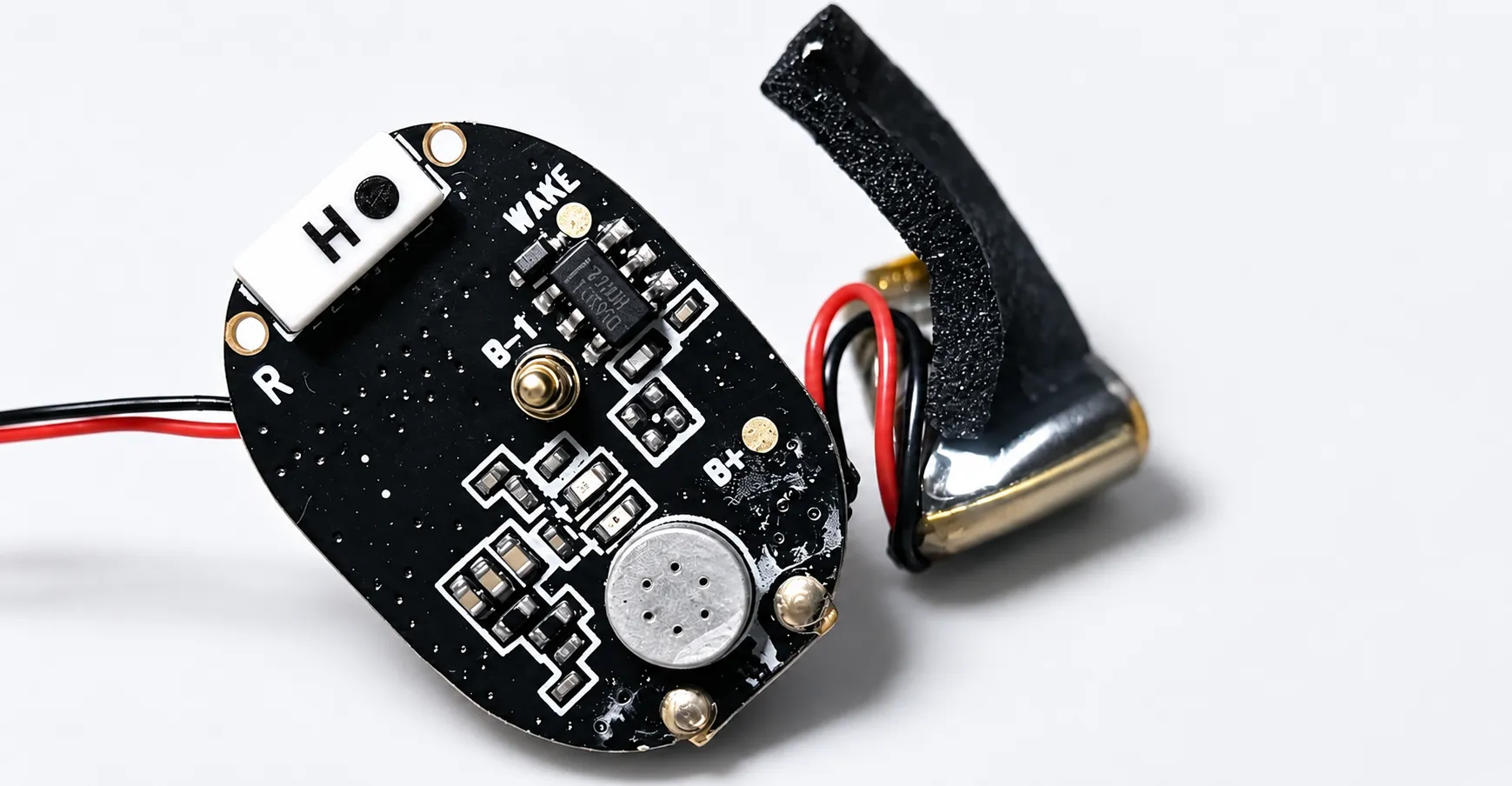
5.1 Ceramic Patch Antennas (Small IoT and Bluetooth Wearable Devices)
Compact in size and highly sensitive, with strict control over clearance and routing:
1. There must be no metal components, traces, or copper foil within 1 mm of the antenna body;
2. All layers of the PCB directly beneath the antenna must be completely clear; ground planes and through-holes are prohibited;
3. The feedline must have a strict impedance of 50 Ω, and the matching circuit must be placed immediately adjacent to the feed point;
4. The distance between the unit’s metal structure and the antenna must be ≥λ/10.
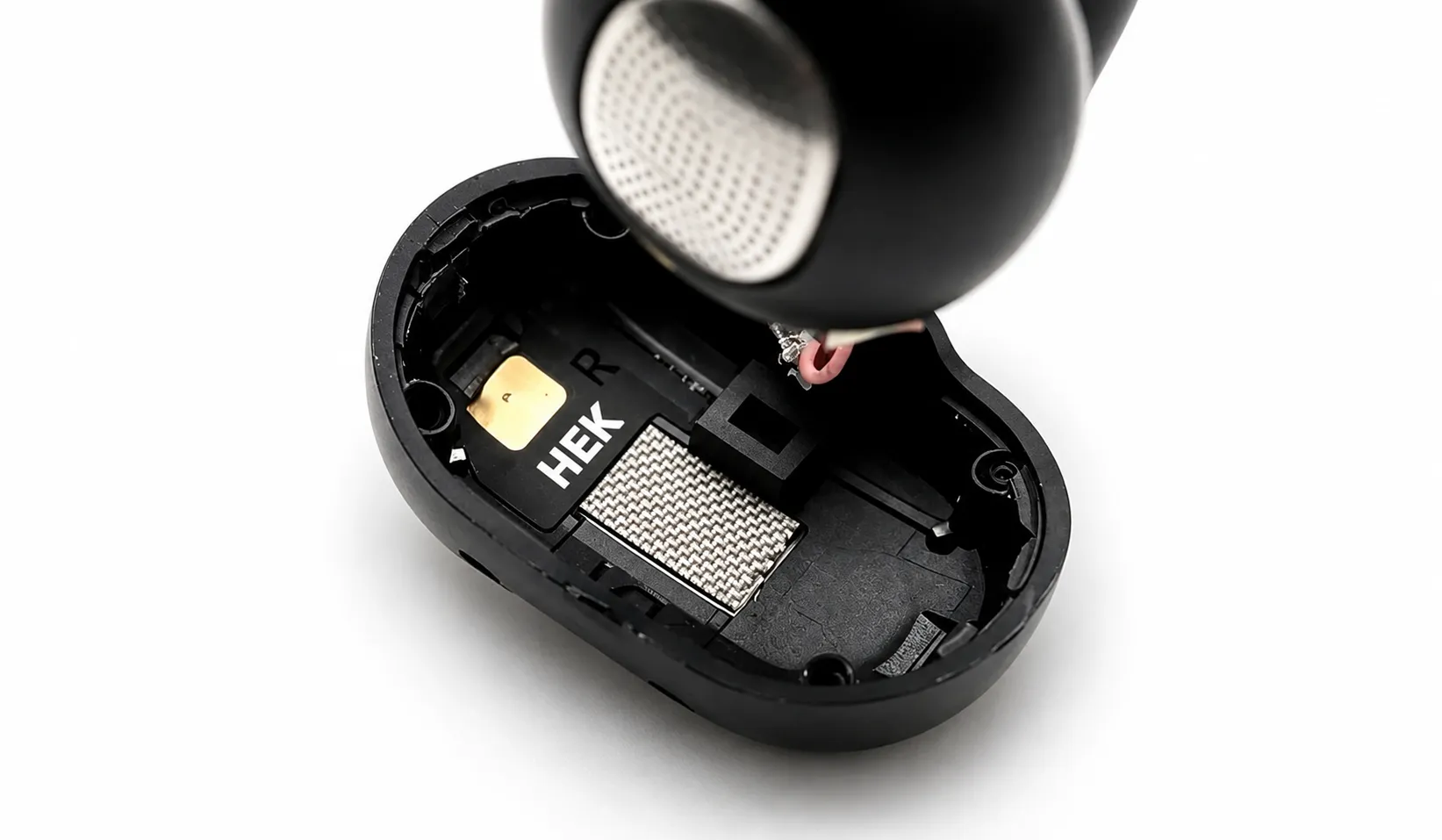
5.2 FPC Flexible Antennas (Smart Wearables, Tablets, Embedded Devices)
Adapted for irregularly shaped structures, ensuring reliable solder pads and complete clearance:
1. Reserve dedicated FPC feed points and ground pads along the edges of the PCB; drill ground vias densely in the ground pads;
2. The PCB area shown in the FPC projection is entirely 3D-clear, with no components, no copper foil, and no screws;
3. Seamless integration of RF traces with the FPC, with a consistent 50Ω impedance throughout and no branches;
In the 4.2.4 GHz band, the distance between the metal battery, the bracket, and the antenna must be ≥12.5 mm;
5. The FPC ground pins must be reliably connected to the PCB ground pads to reduce stray radiation.
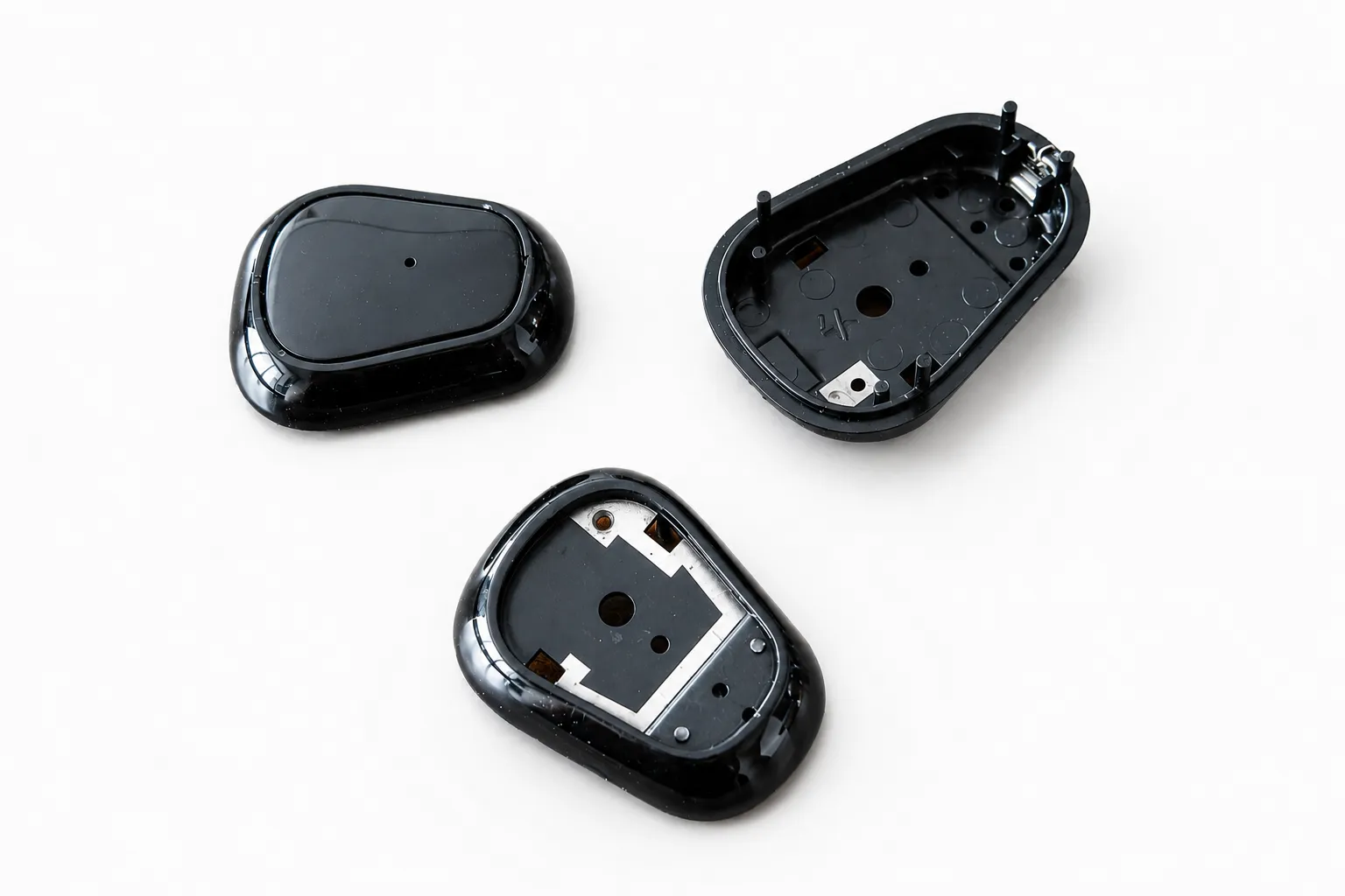
5.3 LDS Laser-Formed Antenna (Smart Device with Metal Frame)
The antenna is molded into the plastic housing; on the PCB side, special attention is paid to controlling the feed point and mitigating metal interference:
1. Dedicated feed and ground pads are reserved along the board edges; the surrounding layers are intact, and multiple vias reduce contact resistance;
2. The board edge area facing the antenna must be kept clear; high-speed digital and power traces must not be routed there;
3. RF traces should be short and straight, with no bends or layer changes, and maintain a 50Ω impedance throughout;
4. Keep the shielding cover, screws, and conductive foam away from the antenna’s projection area to avoid metal coupling interference;
5. The matching circuit is positioned immediately adjacent to the feed point to compensate for impedance shifts caused by the housing and the metal center frame.
VI. Key Points for Avoiding Common Pitfalls in Engineering Projects
1. It is strictly prohibited to place components, shielding frames, or mounting screws within the antenna clearance zone to prevent significant degradation or even failure of antenna performance;
2. Eliminate sudden changes in feedline impedance, frequent changes in layer, and right-angle bends to reduce signal reflection loss;
3. High-speed digital and power traces must not cross RF ground planes to prevent noise from interfering with reception sensitivity;
4. Strictly use single-point grounding to avoid multiple ground connections that could form a ground loop and introduce low-frequency noise;
5. Match the network by reserving a debugging position; do not permanently install a 0Ω resistor, but leave room for impedance tuning;
6. Differentiated Design: The ceramic antenna strictly adheres to the 1mm exclusion zone; the FPC ensures reliable grounding; and the LDS focuses on isolating metal interference.
VII. Conclusion
The core of RF antenna layout can be summarized as follows:Clean power supply for radiation protection, continuous impedance protection, isolation for interference suppression, and stable grounding for noise suppression. In engineering design, it is necessary to first comply with general RF design specifications, then tailor the layout to the specific characteristics of ceramic, FPC, and LDS antennas, balancing structural constraints with electrical performance to prevent RF failures at the source and ensure stable device communication, compliance with range requirements, and excellent interference resistance.